I2C Made Easy: Simplify Your PCB Design with Proven Hardware Tips! How to avoid product failure by design: proven methods to prevent
If you are searching about How to Reduce PCB Crosstalk in Your Layout (Tips) - RayPCB you've visit to the right place. We have 25 Pics about How to Reduce PCB Crosstalk in Your Layout (Tips) - RayPCB like How to Use a Modular Approach to Simplify Your PCB Design Process, 18 PCB Layout Tips for Improving Your PCB Design and Reducing and also PPT - Simplify Your Design with Vertical Launch and Solderless PCB. Here you go:
How To Reduce PCB Crosstalk In Your Layout (Tips) - RayPCB
 www.raypcb.com
How to Reduce PCB Crosstalk in Your Layout (Tips) - RayPCB
How To Avoid Product Failure By Design: Proven Methods To Prevent
 www.unmannedsystemstechnology.com
How to Avoid Product Failure by Design: Proven Methods to Prevent ...
Easy PCB Assembly Tips And Tricks That Will Help Any Beginner - Blog
 www.pcbunlimited.com
Easy PCB Assembly Tips and Tricks That Will Help Any Beginner - Blog ...
Beginner’s Guide To PCB Design: 10 Steps To Craft Your Own Printed
 creatiwise.com
Beginner’s Guide to PCB Design: 10 Steps to Craft Your Own Printed ...
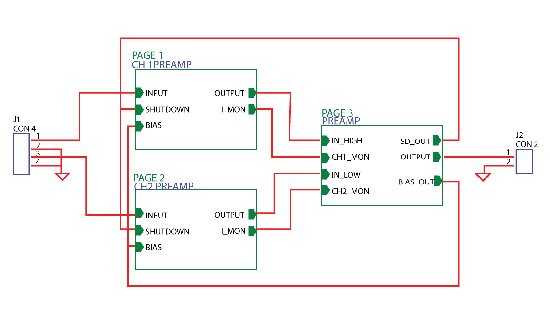
How To Use A Modular Approach To Simplify Your PCB Design Process
 www.linkedin.com
How to Use a Modular Approach to Simplify Your PCB Design Process
PCB Design Engineer Resume Sample (2023)
 itchol.com
PCB Design Engineer Resume Sample (2023)
18 PCB Layout Tips For Improving Your PCB Design And Reducing
 camptechii.com
18 PCB Layout Tips for Improving Your PCB Design and Reducing ...
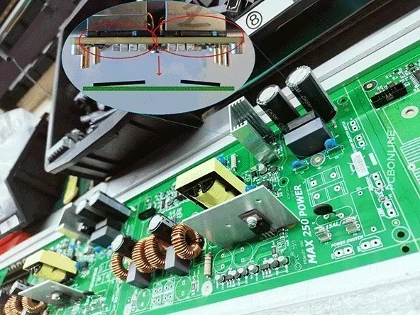
Top Proven Tips For High-Quality Advanced PCB Assembly
 www.pcbonline.com
Top Proven Tips for High-Quality Advanced PCB Assembly
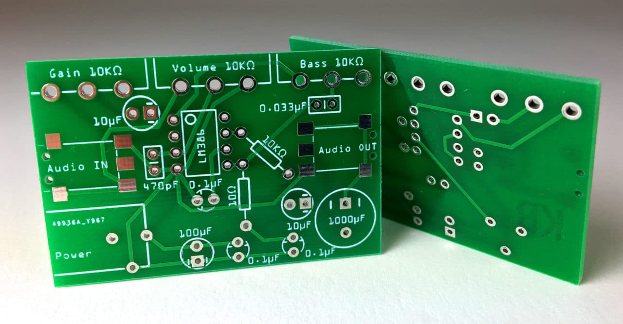
PCB Components- 14 Important Tips For Choosing PCB Components
 www.wellpcb.com
PCB Components- 14 Important Tips for Choosing PCB Components
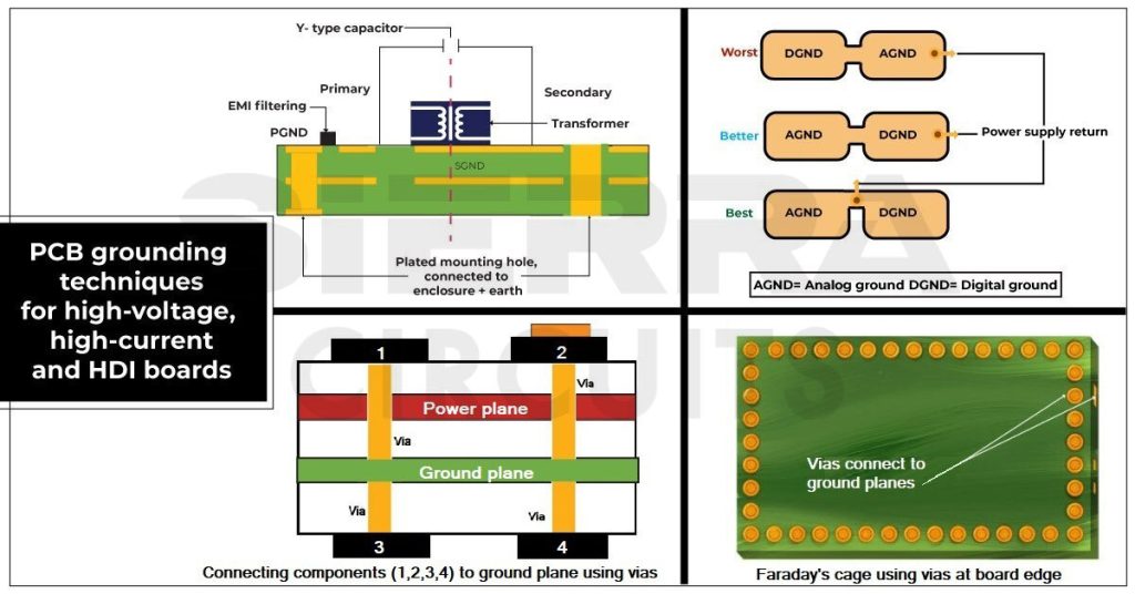
Tips And PCB Design Guidelines For EMI And EMC Sierra Circuits
 www.designinte.com
Tips And PCB Design Guidelines For EMI And EMC Sierra Circuits ...
PCB Design – Riosh Technologies
 www.rioshtech.com
PCB Design – Riosh Technologies
Power Supply PCB Design Guidelines For Manufacturing - VSE
 www.vse.com
Power Supply PCB Design Guidelines for Manufacturing - VSE
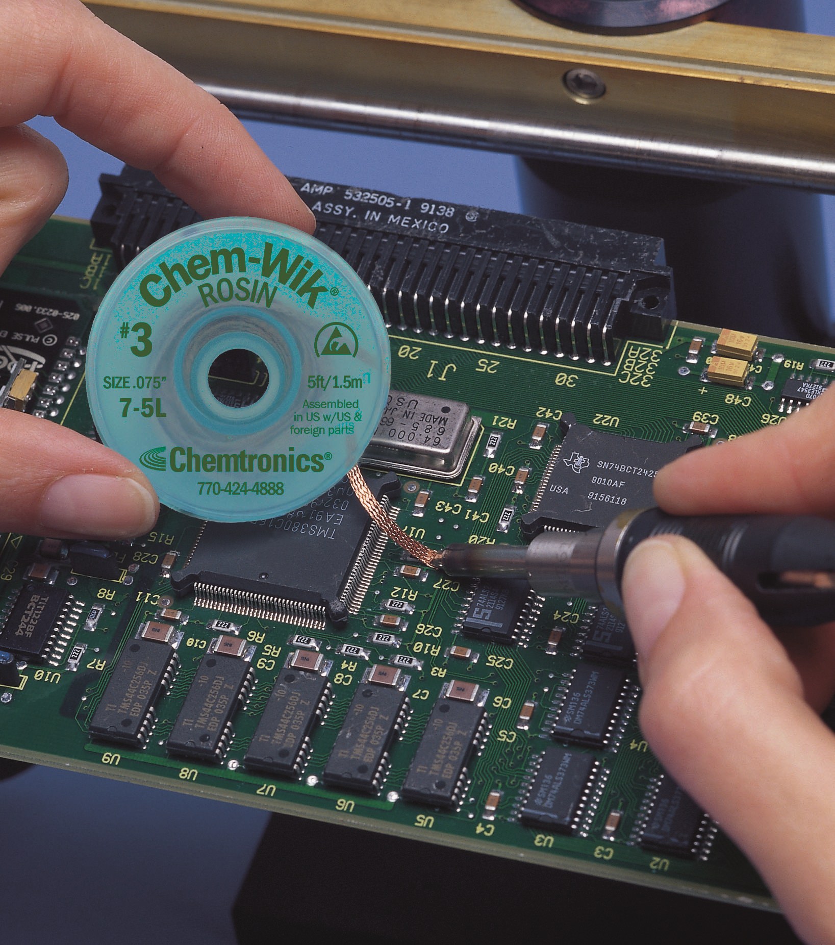
12 Easy Tips To Improve Your PCB Desoldering Process Today | Chemtronics
 www.chemtronics.com
12 Easy Tips to Improve Your PCB Desoldering Process Today | Chemtronics
Mastering The Art Of PCB Design Basics | Sierra Circuits
 www.protoexpress.com
Mastering the Art of PCB Design Basics | Sierra Circuits
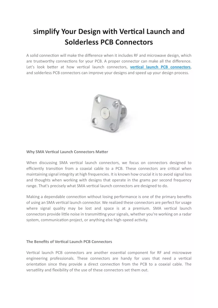
PPT - Simplify Your Design With Vertical Launch And Solderless PCB
 www.slideserve.com
PPT - Simplify Your Design with Vertical Launch and Solderless PCB ...
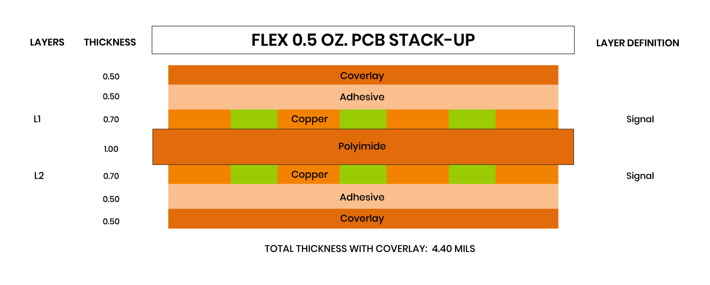
PCB Stack-Up Guide & Examples | San Francisco Circuits
 www.sfcircuits.com
PCB Stack-Up Guide & Examples | San Francisco Circuits
Pcb Layout And Thermal Design Techniques For High Den - Vrogue.co
 www.vrogue.co
Pcb Layout And Thermal Design Techniques For High Den - vrogue.co
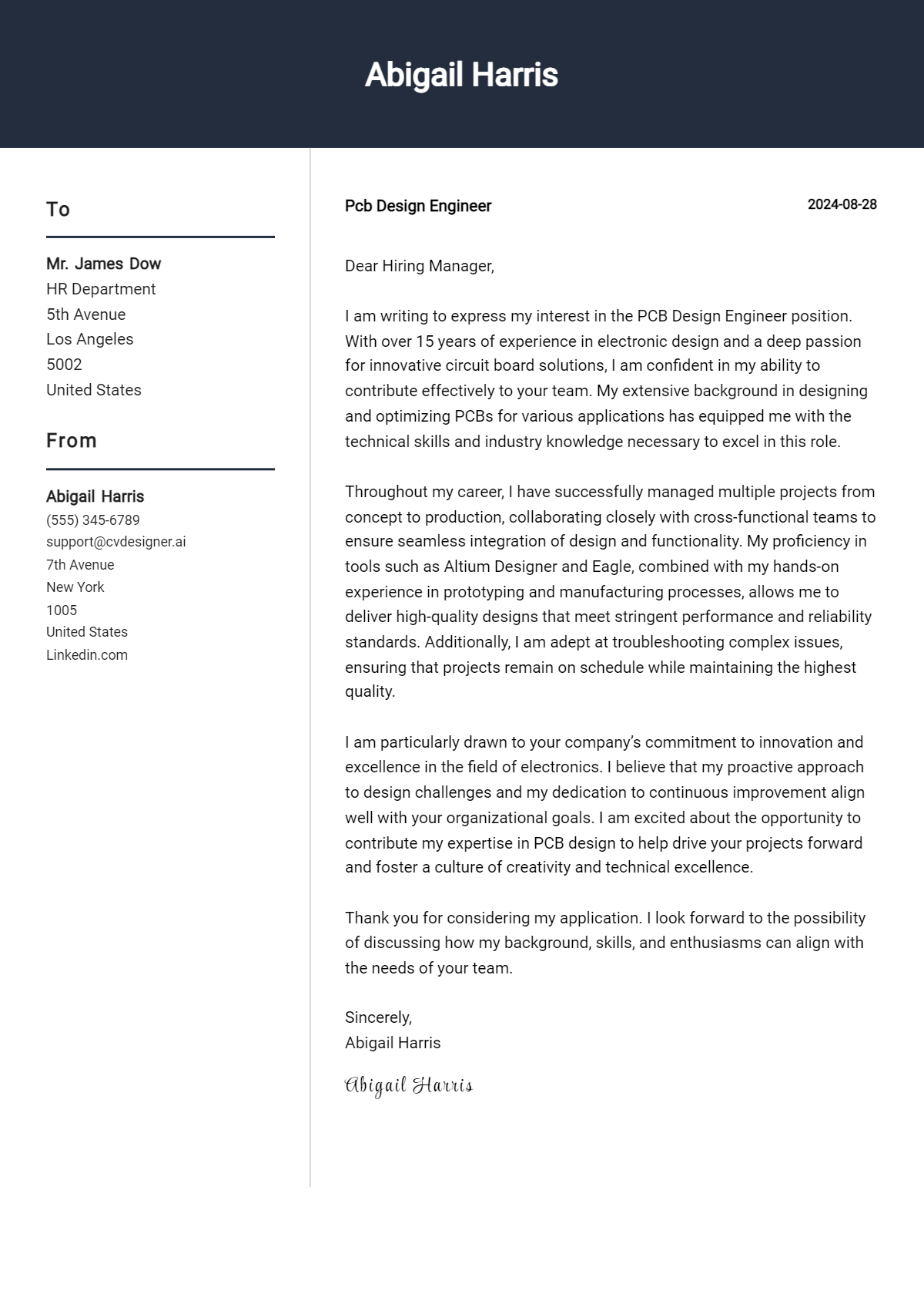
PCB Design Engineer Cover Letter Example For 2024: Proven Tips
 cvdesigner.ai
PCB Design Engineer Cover Letter Example for 2024: Proven Tips ...
Design For Better Signal Integrity By Rick Hartley | Sierra Circuits
 www.protoexpress.com
Design for Better Signal Integrity by Rick Hartley | Sierra Circuits
What Determines The PCB Cost? How To Reduce It? - MOKO
 www.mokotechnology.com
What Determines the PCB Cost? How to Reduce It? - MOKO
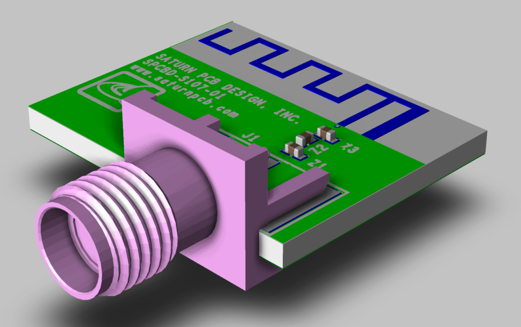
How To Design A PCB Antenna?
 www.nextpcb.com
How to Design a PCB Antenna?
Top Proven Tips For High-Quality Advanced PCB Assembly
 www.pcbonline.com
Top Proven Tips for High-Quality Advanced PCB Assembly
Pcb Printers - Egpsawe
 egpsawe.weebly.com
Pcb printers - egpsawe
Pcb Design Tips For Beginners - Design Talk
 design.udlvirtual.edu.pe
Pcb Design Tips For Beginners - Design Talk
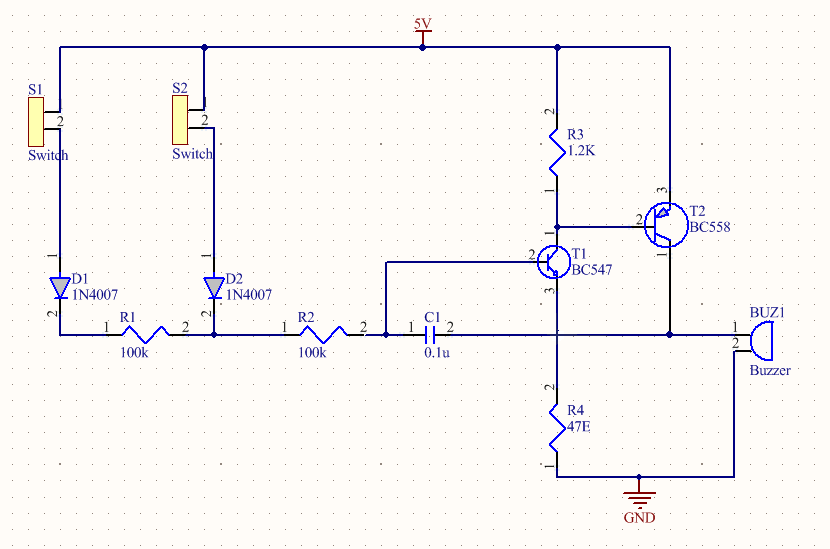
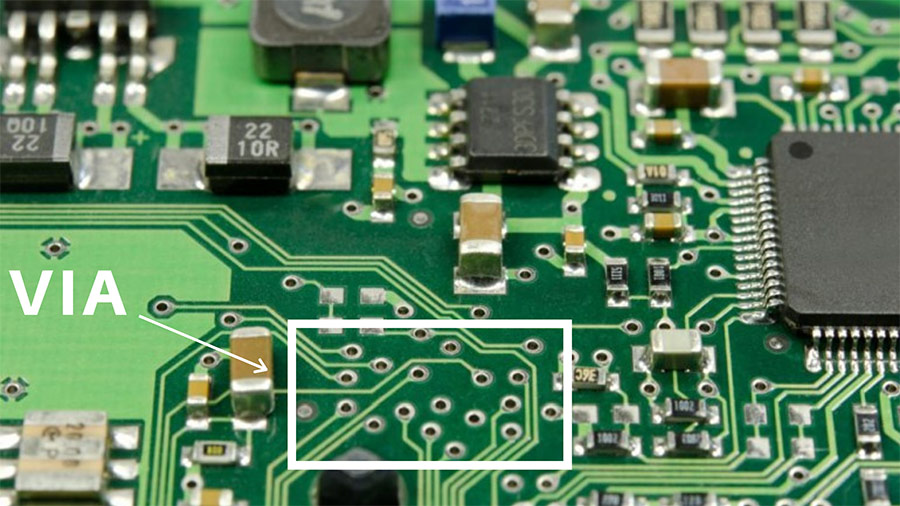
What Is Via In PCB Design And How To Use Them - Gadgetronicx
 www.gadgetronicx.com
What is Via in PCB design and how to use them - Gadgetronicx
12 easy tips to improve your pcb desoldering process today. How to use a modular approach to simplify your pcb design process. How to design a pcb antenna?